
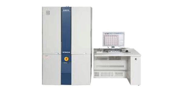
SU9000 II
Ultra-high Resolution Scanning Electron Microscope
The CFE Gun technology featured in the SU9000 achieves the highest SEM resolution in the world. (0.4nm at 30kV).
The SU9000II is ideal for high-resolution imaging with a small source size and energy spread. It features unique electron optics, with the sample positioned inside a gap between the upper and lower parts of the objective lens pole piece. With his innovative cold field emission gun technology guarantees the highest possible system resolution (SE resolution 0.4 nm à 30 kV, 0.7 nm à 1kV with deceleration feature) and the highest stability against external disturbances (fields, vibrations, contamination).
SU9000II uses an ultra-stable side-entry stage similar to high-end TEM systems and incorporates optimized vibration damping and a closed cabinet to shield the electron optics from environmental noise.
Furthermore, the clean vacuum concept of the SU9000II offers a vacuum level in the gun and sample chamber that is one order of magnitude than previous generation, minimizing sample contamination artefacts.
New features have been added like to allow automatic adjustments of optical system and the EM Flow Creator software package as an option for automated data acquisition, particularly sequential data collection.
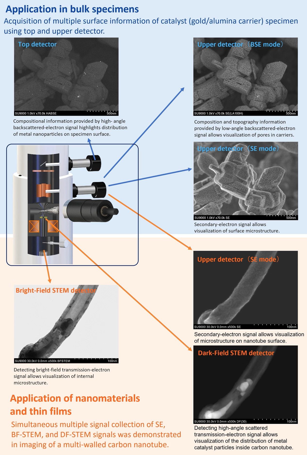
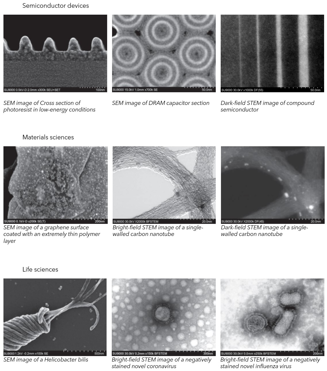
Application
Features and variations
- The world’s highest SE resolution: 0.4nm at 30kV
- New designed Cold field-emission electron gun allowing both high brightness and an extremely stable emission current
- Superior low kV performance for observing beam sensitive materials. SE resolution: 0.7nm at 1kV landing voltage (with deceleration option)
- Ultrahigh vacuum specimen chamber reducing sample contamination artefacts
- High-rigidity frame and acoustic enclosure ensuring high-performance operation under a wide variety of environments
- New LV STEM capabilities: the position of the BF/DF Duo STEM can be regulated to control the detection of scattering signal from low to high angle in dark-field mode. Low aberration in-lens objective lens and optical system optimized for STEM observations. Lattice images can be observed in SEM/STEM
Características y Variaciones
- La resolución SE más alta del mundo: 0.4 nm a 30 kV.
- Nueva cañón de electrones de emisión de campo frío rediseñado que permite tanto alta brillantez como una corriente de emisión extremadamente estable.
- Rendimiento superior a bajo kV para observar materiales sensibles al haz. Resolución SE: 0.7 nm a 1 kV de voltaje de aterrizaje (con opción de desaceleración).
- Cámara de muestra de ultravacío que reduce los artefactos de contaminación de la muestra.
- Estructura de alta rigidez y recinto acústico que aseguran un funcionamiento de alto rendimiento en una amplia variedad de entornos.
- Nuevas capacidades LV STEM: la posición del Duo STEM BF/DF puede regularse para controlar la detección de señales de dispersión desde ángulos bajos hasta altos en modo de campo oscuro. Lente objetivo in-lens de baja aberración y sistema óptico optimizado para observaciones STEM. Las imágenes de red se pueden observar en SEM/STEM.